Printed Circuit Boards
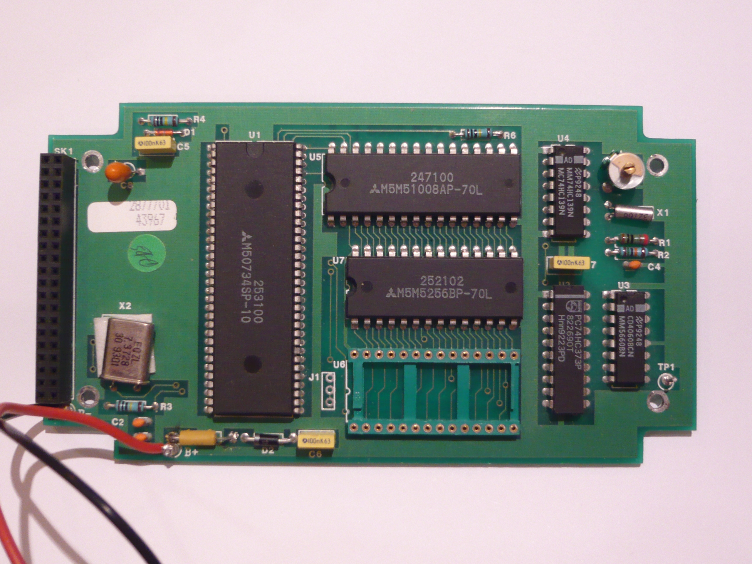
The Monolog electronics comprise two double-sided PCBs, stacked and interconnected via a 40-pin header. The upper board carries all the analogue circuitry; the lower board carries all the digital circuitry. Both boards are fitted inside the Monolog enclosure regardless of hardware mark — the same electronics are used throughout all three enclosure variants.
| Board | Layer count | Function |
|---|---|---|
| Upper — Analogue | 2-layer | Modem, line interface buffers, DTMF decoder, RS-232 components, 25-way D-type connector |
| Lower — Digital | 2-layer | CPU, RAM, ROM/EPROM, reverse battery protection, real-time clock |
RAM Configurations
Units were shipped in three RAM configurations. Call storage capacity varies with call content — outgoing calls consume more memory than incoming.
| Configuration | Total RAM | Typical Capacity |
|---|---|---|
| (i) Standard | 32K | ~2,000 calls |
| (ii) Extended | 32K + 32K | ~4,000 calls |
| (iii) Maximum | 32K + 128K | ~10,000 calls |
Once RAM is full, Monolog overwrites the oldest records first. Data is never lost mid-call — the buffer only advances at call boundaries.
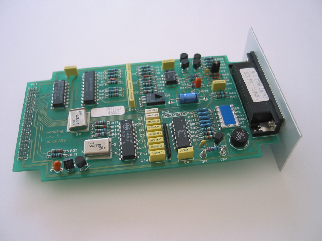
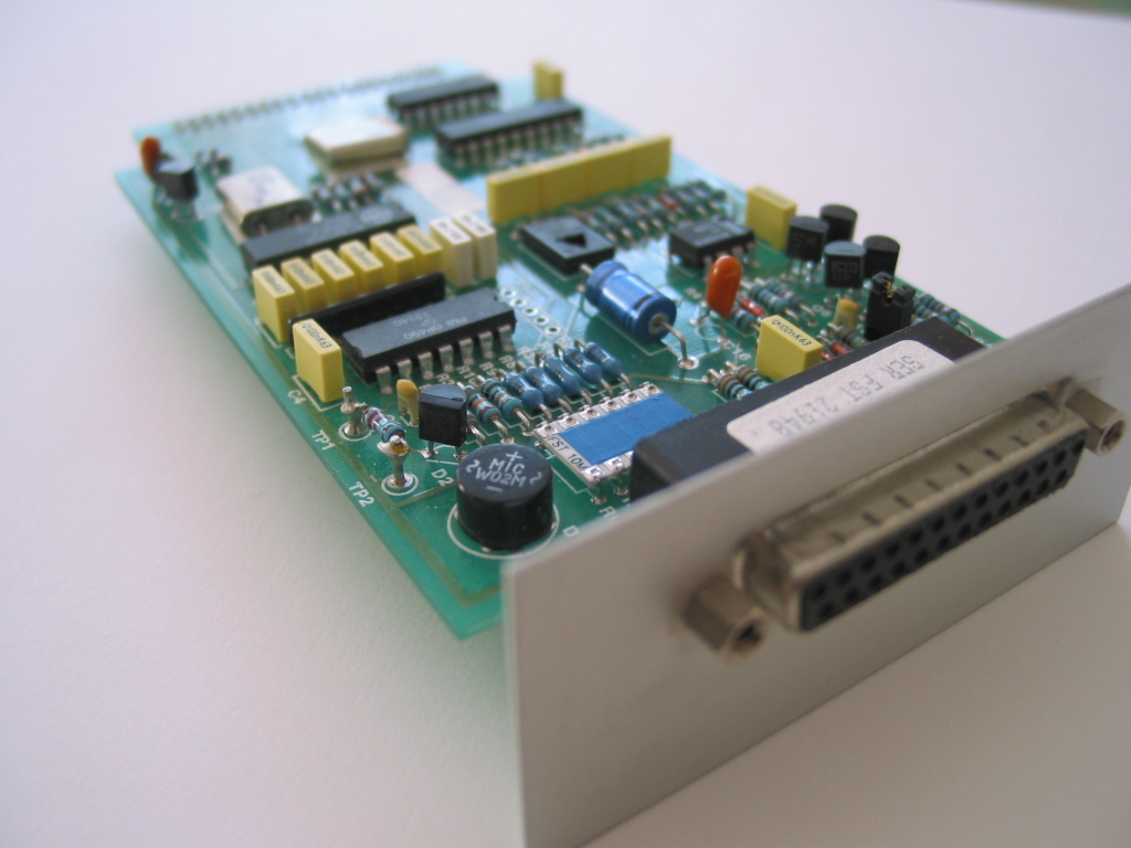
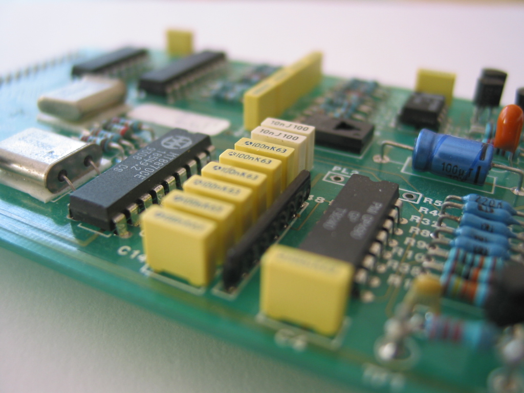
Analogue PCB
The upper analogue board handles all interaction with the telephone line and the external world. Key components visible on the board include the modem IC, DTMF decoder, RS-232 level converter, the bank of yellow polyester capacitors forming the line interface filter network, and the 25-way D-type connector at the front edge which provides both the RS-232 port (Mark II) and the line connections.
Two test points — TP1 and TP2 — are provided for calibrating the voltage reference IC (D2), allowing the correct resistor value to be selected and installed during manufacture.
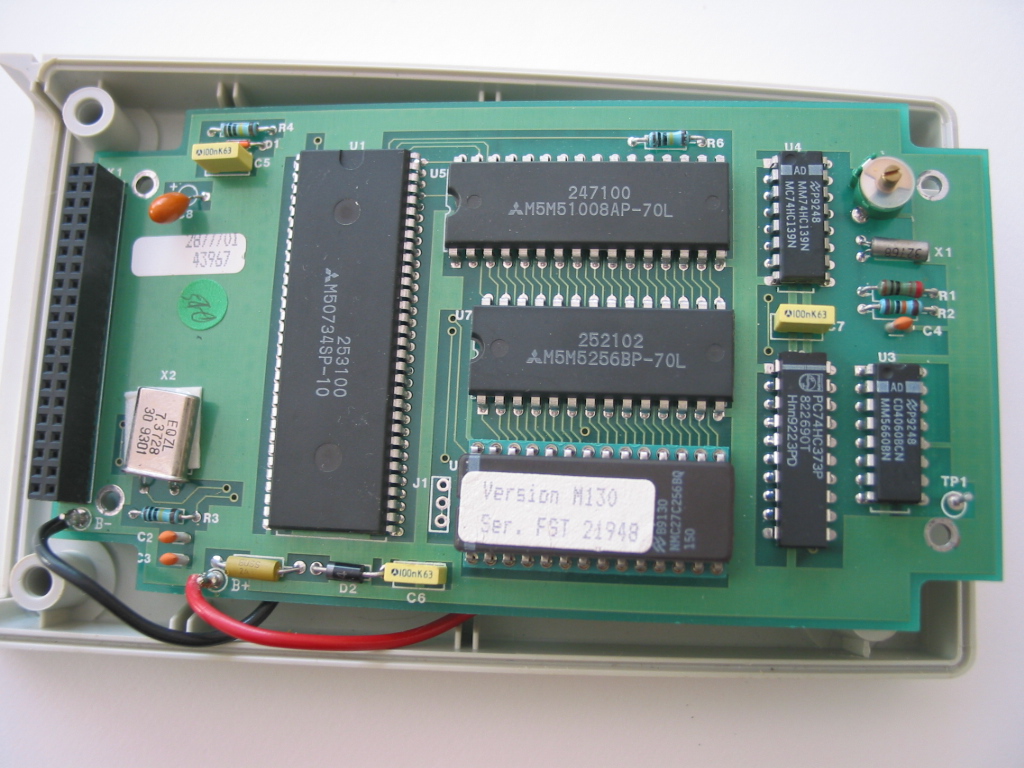
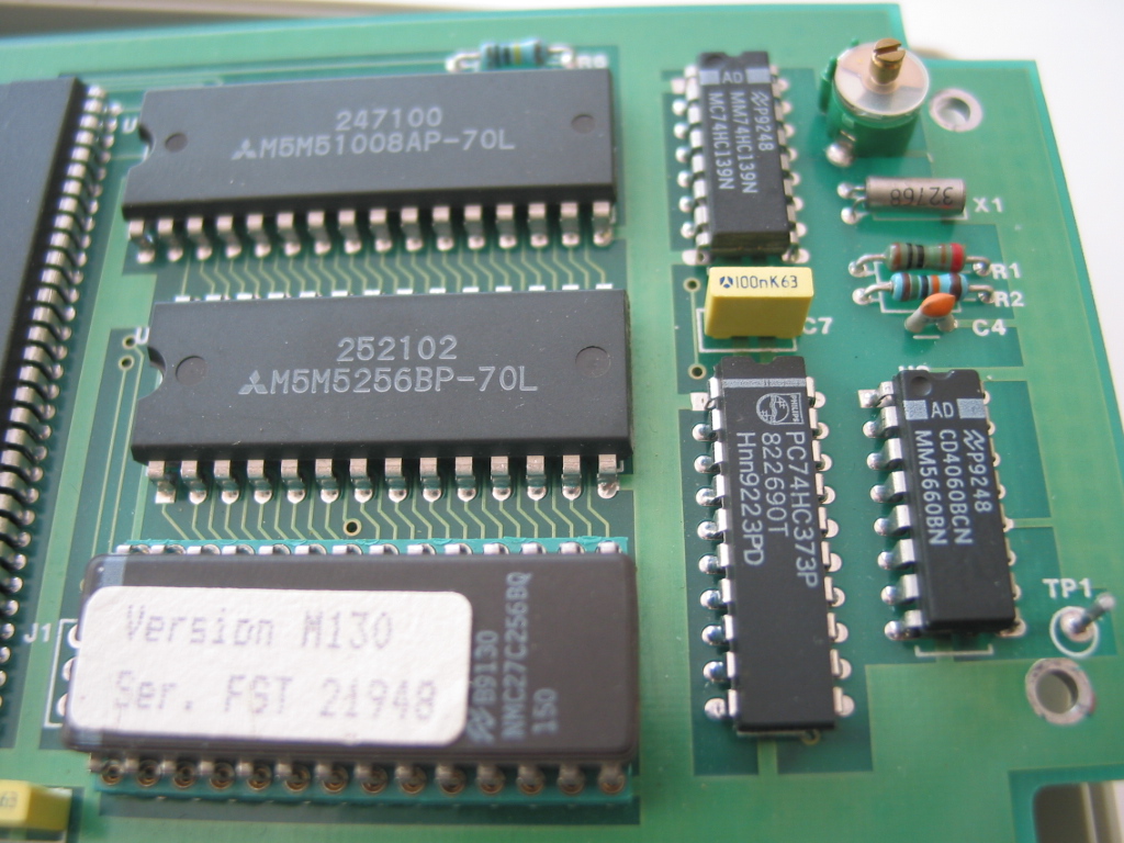
Digital PCB
The lower digital board carries the core processing and storage electronics. The Mitsubishi M50734SP-10 — an enhanced 6502-series processor with on-chip I/O, UART and A/D converter — forms the heart of the design. RAM is provided by one or two Mitsubishi M5M51008AP-70L (32K×8) chips with an optional M5M5256BP-70L (32K×8) for the extended configuration. The firmware EPROM sits in a ZIF or standard socket at the centre of the board, clearly labelled with version and serial number. A 7.3728 MHz oscillator (X2) provides the CPU system clock. A separate 32.768 kHz oscillator (X1) drives the real-time clock divider chain.
Calibration
Two calibration procedures were performed during manufacture of each unit, one on each board.
Analogue Board — Voltage Reference (D2)
Test points TP1 and TP2 on the analogue board allow measurement of the output of the voltage reference IC (D2). The reading taken determines the correct value of resistor to fit, ensuring the A/D converter inputs are correctly scaled for battery and line voltage measurement.
Voltage Reference Calibration Photo
Photo to be added — TP1/TP2 measurement on analogue board
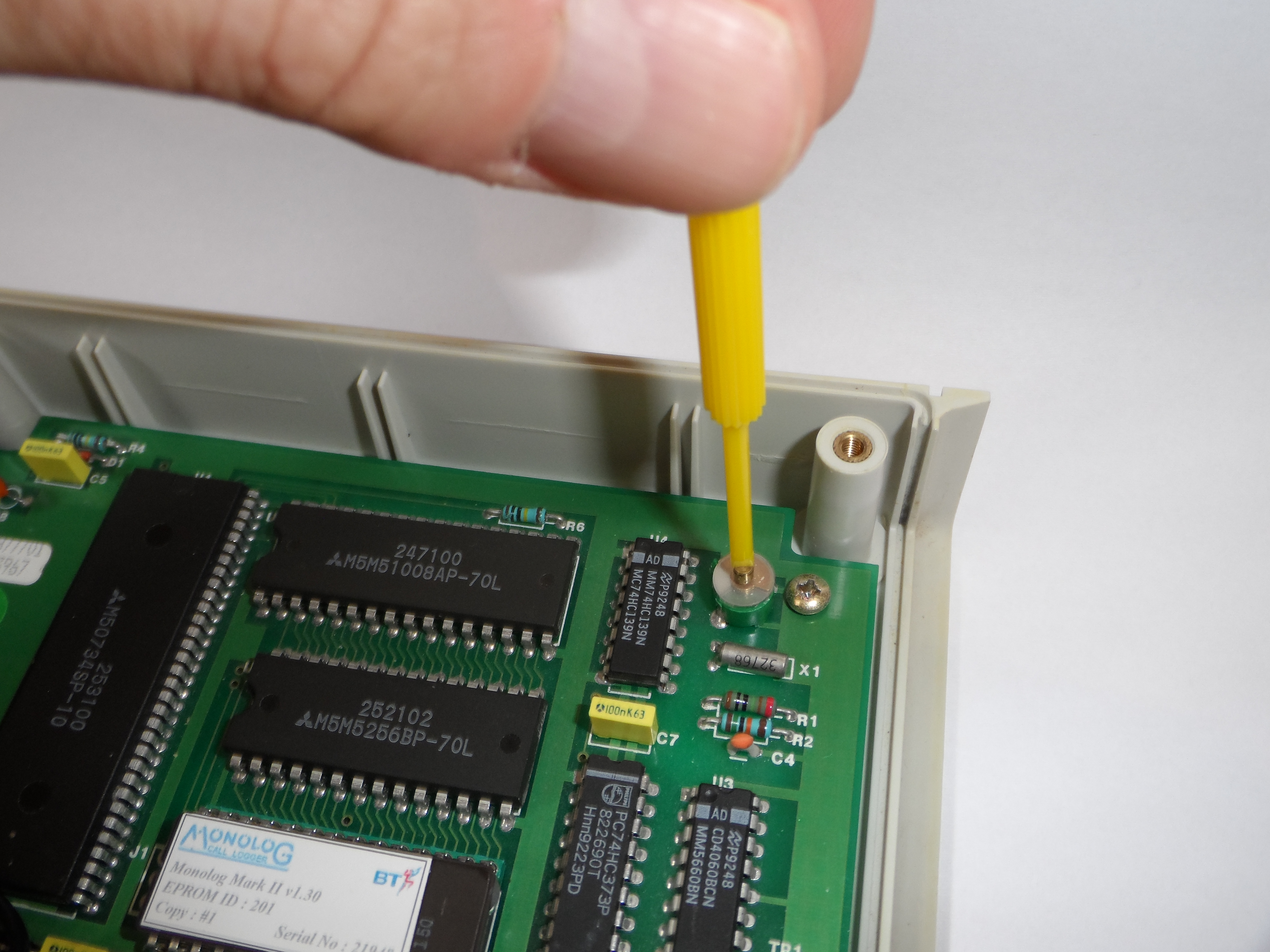
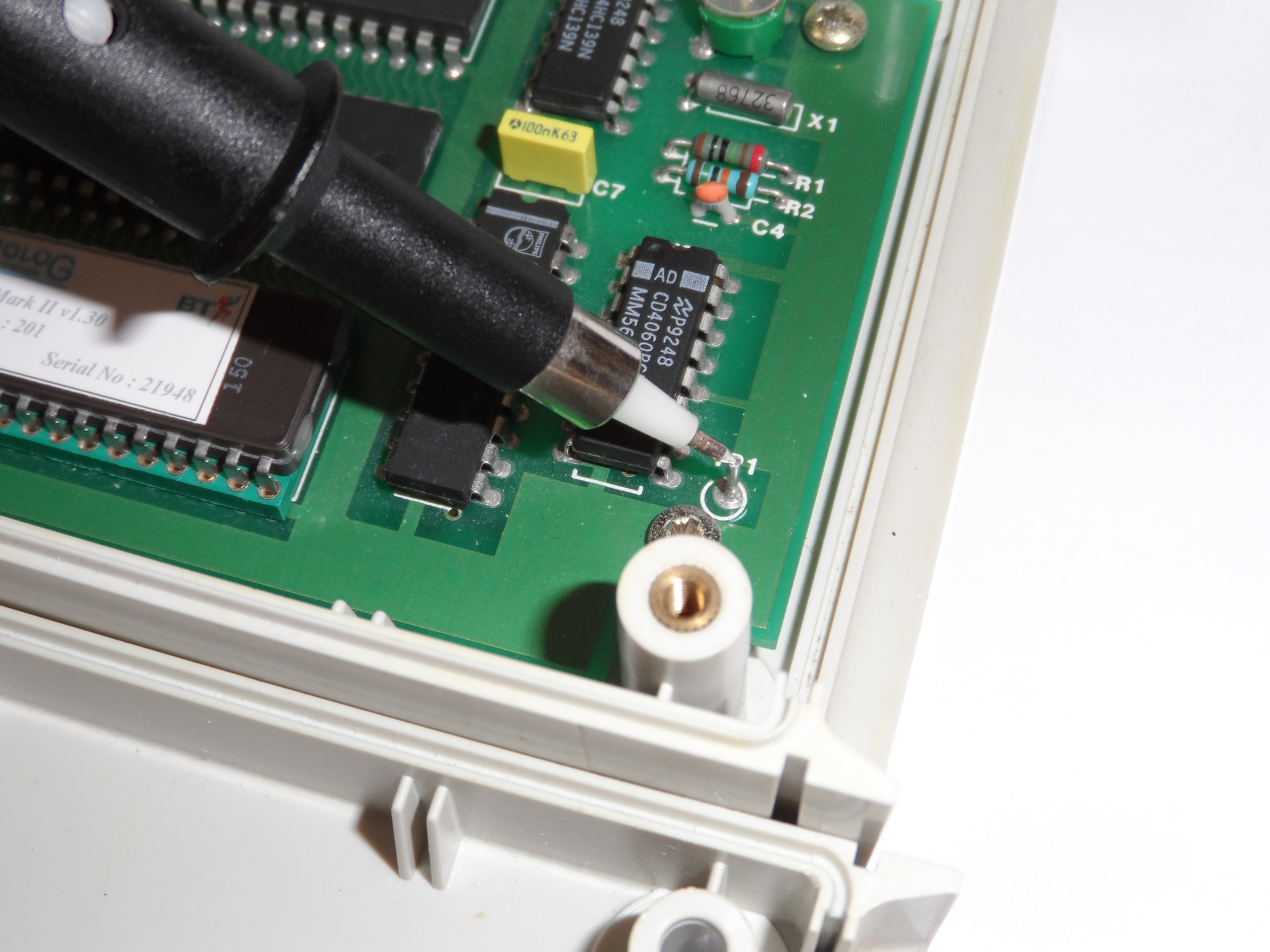
Digital Board — Real-Time Clock
Two steps are performed on the digital board to set the real-time clock accurately. First, a trimmer potentiometer is adjusted to bring the clock frequency as close as possible to the target. Second, a test point connected to a spare output pin of the CMOS divider IC (CD4060) allows the resulting frequency to be verified directly with a frequency meter. Clock accuracy of ≤ 1 second per day is the target.
SPM Daughter Board — Unconfirmed Development
The information in this section is based on evidence within the Monolog hardware and firmware, combined with original documentation references. No production example of this board has been found or confirmed to exist.
The Monolog documentation of the period refers to the development of an internal plug-in module intended to detect 12/16 kHz Subscribers Private Meter (SPM) pulses directly — without the need for an external SPM connection at the MIU. The analogue PCB carries an unused 5-way connector (PL2) which appears to have been designed specifically to accommodate this future development, providing the necessary power, ground and signal connections for a daughter board.
Within the firmware, one of the options for the PULSES command — PULSES SPM16 — is reserved to switch Monolog into a mode that makes use of this board. The command exists in the command set but its practical effect depends entirely on the daughter board being present.
Physical Constraints
Any such board would have had to be very compact. With the analogue PCB fitted inside the Monolog enclosure, the clearance between the top surface of the PCB and the underside of the plastic lid is minimal — the daughter board would need to sit within that gap, plugging vertically or at a low angle into PL2.
Proposed Circuit
The schematic below represents a plausible implementation based on the CMX631A Low Voltage SPM Detector IC — a device well-suited to this application. It detects 12 or 16 kHz tone bursts on the monitored line and provides a clean digital output to the CPU. Whether this reflects the original designer's intent is not known.
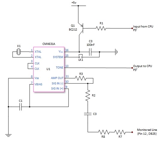
| Signal | Connection | Description |
|---|---|---|
| Monitored Line | Pin 12, DB25 | Line input — 12/16 kHz SPM tone bursts detected here |
| Input from CPU | P3' | CPU controls Q1 (BC212) to enable/disable the CMX631A SYSTEM pin |
| Output to CPU | P3' | TONE output from CMX631A — digital pulse output for each detected meter event |
| LK1 | On-board link | Selects 12 kHz or 16 kHz detection mode |
| PL2 | Analogue PCB | 5-way connector on analogue board — power, ground and signal interface to daughter board |
If you have any knowledge of whether this board was ever produced, or have encountered one in the field, it would be very welcome information for this documentation.
Key Components
| Reference | Device | Function | Board |
|---|---|---|---|
| U1 | Mitsubishi M50734SP-10 | Enhanced 6502 CPU with on-chip I/O, UART, A/D converter | Digital |
| U5 | Mitsubishi M5M51008AP-70L | 128K×8 SRAM (used as 32K×8 via paging) | Digital |
| U7 | Mitsubishi M5M5256BP-70L | 32K×8 SRAM — additional RAM option | Digital |
| U6 | 27C256 / NMC27C256BQ | 32K×8 EPROM — firmware | Digital |
| X1 | 32.768 kHz oscillator | Real-time clock reference | Digital |
| X2 | 7.3728 MHz oscillator | CPU system clock | Digital |
| U3 | CD4060BCN | 14-stage ripple counter / divider — RTC chain | Digital |
| U4 | MM74HC139N / MC74HC139N | Dual 2-to-4 line decoder — address decoding | Digital |
| D2 | MTC2W02M (Zener / ref) | Voltage reference for A/D calibration | Analogue |
| TP1, TP2 | Test points | Voltage reference calibration measurement | Analogue |
| TP1 | Test point | RTC frequency measurement point (CD4060 output) | Digital |